A Motivating Question: What Do We Want Computers to Do?
At its core, a computer is a machine that performs computations. To do this, it needs to accomplish a few fundamental tasks:
- Represent Data: We need a way to encode information, whether it's numbers, text, or images, into a format the machine can understand.
- Control Data Flow: We need to be able to direct the flow of this information, sending it where it's needed for processing or storage.
- Manipulate Data: We need to be able to perform operations on the data, like arithmetic or logical comparisons, to produce a result.
Throughout history, brilliant minds have explored various ways to build these computational machines. Early attempts included mechanical computers, like Blaise Pascal's adding machine, which used gears and wheels. There were also analog computers, which represented numbers with continuous physical quantities like voltage or rotation. While these machines were groundbreaking for their time, they were often slow, imprecise, and limited in their capabilities.
The advent of electronics brought about the era of digital computers. These machines represent data using discrete values, typically binary digits (bits), which are like tiny on/off switches. This approach proved to be far more powerful and scalable. The journey to the modern digital computer, however, was a long one, with each new generation of technology bringing us closer to the powerful devices we have today.
Prerequisites
Think of electricity as water flowing through pipes.
- Voltage is like the water pressure. It's the potential difference that "pushes" the electric charge. Voltage is always measured between two points.
- Current is the actual flow of electric charge, like the flow of water. For current to flow, there must be a closed loop, or circuit.
In digital electronics, we use two distinct voltage levels to represent the binary values 0 and 1. We might say, for example, that 0 volts represents a "low" signal (binary 0) and 5 volts represents a "high" signal (binary 1). The exact voltages don't matter as much as the clear distinction between "high" and "low".
The key to the transistor lies in a material called a semiconductor, most commonly silicon. In a pure silicon crystal, each atom is bonded to its neighbors, and there are no free electrons to carry a current. This is where a process called doping comes in.
- N-type Semiconductor: If we add a small amount of an element with five valence electrons (like phosphorus) to the silicon lattice, there will be extra electrons that are free to move around. Since electrons have a negative charge, we call this N-type (Negative) silicon.
- P-type Semiconductor: If we add an element with three valence electrons (like boron), there will be "holes" where an electron is missing. These holes can be thought of as positive charge carriers, so we call this P-type (Positive) silicon.
When we join a piece of P-type silicon with a piece of N-type silicon, we create a P-N junction. At the junction, the free electrons from the N-type side are attracted to the holes on the P-type side and they combine. This creates a depletion region at the junction where there are no free charge carriers. This region acts as a barrier, preventing current from flowing easily across the junction.
Transistors
The most common type of transistor used in modern computer chips is the Metal-Oxide-Semiconductor Field-Effect Transistor, or MOSFET. MOSFETs come in two main "flavors": NFETs and PFETs.
A MOSFET has three main parts:
- Source: The source of the charge carriers (electrons for NFETs, holes for PFETs).
- Drain: Where the charge carriers flow to.
- Gate: This acts as a switch that controls the flow of charge between the source and the drain.
The gate is separated from the semiconductor material by a very thin layer of insulating material, usually silicon dioxide.
Here's a simplified look at how an NFET works: We start with a P-type silicon substrate. Within this substrate, we create two N-type regions for the source and the drain. Normally, no current can flow between the source and drain because of the P-type material in between. When we apply a positive voltage to the gate, it creates an electric field that attracts electrons to the area under the gate. If the gate voltage is high enough, it attracts enough electrons to create a thin "channel" of N-type material connecting the source and the drain. Now, current can flow freely from the source to the drain. The transistor is "on". When we remove the positive voltage from the gate, the channel disappears, and the flow of current stops. The transistor is "off".
![]() Credit to CMOS VLSI Design: A Circuits and Systems Perspective
Credit to CMOS VLSI Design: A Circuits and Systems Perspective
A PFET works in a similar but opposite way. It has a P-type channel on an N-type substrate, and it is turned on by a negative voltage at the gate.
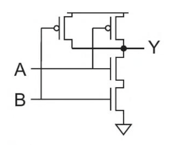
Building a Simple NAND Gate with Transistors
Now for the really cool part: we can combine these simple transistor switches to perform logic operations. Let's build a simple NAND gate. A NAND gate outputs a "1" only if both of its inputs are "0".
We can create an NAND gate using a combination of NFETs and PFETs in a structure called CMOS (Complementary Metal-Oxide-Semiconductor).
Pull-Down Network: This part of the circuit is made of NFETs and is designed to pull the output voltage down to "low" (0) under certain conditions. For an NAND gate, we connect two NFETs in series between the output and the ground.
Pull-Up Network: This part is made of PFETs and is designed to pull the output voltage up to "high" (1). For an NAND gate, we connect two PFETs in parallel between the power supply and the output.
 Credit to CMOS VLSI Design: A Circuits and Systems Perspective
Here's how it works:
Case 1: At least one input is "low" (0)
If either input A or input B (or both) is "low" (0), the following occurs: At least one of the PFETs in the parallel pull-up network will turn on, creating a path from the output to the high voltage supply (Vdd). At least one of the NFETs in the series pull-down network will be off, breaking the path to ground. As a result, the output is pulled "high" (1).
Case 2: Both inputs are "high" (1)
When both input A and input B are "high" (1): Both NFETs in the series pull-down network turn on, creating a direct path from the output to the ground. Both PFETs in the parallel pull-up network will turn off. Consequently, the output is pulled "low" (0). This behavior makes the NAND gate a "universal gate," meaning that any other logic gate (like AND, OR, and NOT) can be constructed using only NAND gates.
Why can't NFETs be in the pull-up network? NFETs are good at pulling the output down to ground, but they are not very efficient at pulling the output all the way up to the high voltage supply. They would cause a voltage drop, leading to a "weak" high signal. PFETs, on the other hand, are excellent at pulling the output up to the high voltage. This is why we use a complementary pairing of NFETs for the pull-down and PFETs for the pull-up network.
By combining transistors in this way, we can create all the fundamental logic gates (AND, OR, NOT, etc.) that are the building blocks of modern microprocessors and computer chips. From these simple switches, we build the complex digital world we live in.
Bonus Material: Saturation and Linear Regimes
MOSFETs have different operating modes, but for digital circuits, we primarily use them as switches, operating in two main regions:
Cut-off Region: When there is no voltage on the gate, the transistor is off, and no current flows.
Linear (or Triode) Region: When the transistor is turned on, it acts like a resistor, and the current flow is proportional to the voltage between the drain and source.
Saturation Region: In this mode, the current from the drain to the source becomes relatively constant, regardless of the voltage between them. The transistor acts more like a constant current source.
For digital logic, we want the transistor to be either fully off (cut-off) or fully on (in the linear region, acting as a switch with low resistance).